Turns out that CPU clocks can actually be increased by modifying the OPP tables in firmware - they are not hardcoded as I initially thought. Here’s a rough guide:
Clone the edk2, edk2-platforms and edk2-non-osi repositories from Radxa Computer · GitHub and follow the build instructions in edk2-non-osi/Platform/CIX/Sky1/Readme.md
Copy edk2-non-osi/Platform/CIX/Sky1/PackageTool/pm_config/ to edk2-platforms/Platform/Radxa/Orion/O6/pm_config/
Open opp_config_custom.h inside the copied pm_config directory
Set #define PM_OPP_TABLE_CONFIG 1
Tweak the frequency and voltage levels in the defined OPP tables (at your own risk!)
dxs_lit - little cluster
dxs_gb0 - big cluster 0
dxs_gb1 - big cluster 1
dxs_gm0 - medium cluster 0
dxs_gm1 - medium cluster 1
Rebuild and flash the generated firmware
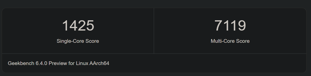
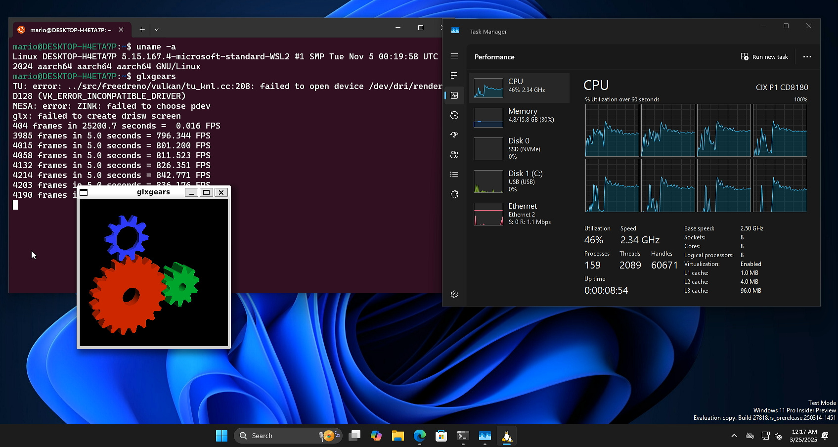
Here’s a GB6 run with the big clusters set to 2.8, medium to 2.4 and little to 1.8 GHz:
While playing with the firmware, I also noticed that there’s support for the fastboot protocol:
You will need to have an NVME drive plugged in (we won’t be writing anything to it), otherwise the fastboot app will refuse to load.
Open your build_and_package.sh:
add local FASTBOOT_LOAD=nvme
append -D TOKEN_SETUP_SUPPORT=TRUE to the EDK2 build command
Build and flash the generated firmware as usual.
There will appear a new setup menu: CIX System Manager. Open it, then go to Soc Configuration->USB Configuration and switch USBC DRD Controller Role to Device. Save the changes.
While rebooting/powering the board, short the “BOOT” pins near the UART debug headers. This will cause the firmware to enter fastboot mode after the boot countdown:
From now on, you can update the firmware by simply running fastboot flash bootloader PATH_TO_FW.bin in a terminal / command prompt.
Reboot the board (fastboot reboot).
To further speed up testing, it’s possible to flash individual parts of the firmware image.
In the case above where we modified the OPP tables, it was only necessary to update csu_pm_config.bin.
edk2-non-osi/Platform/CIX/Sky1/PackageTool/spi_flash_config_ota.json contains a single entry for the EDK2 BL33 image (bootloader3.img). Replace it with the definition for csu_pm_config.bin taken from spi_flash_config_all.json.
Build the firmware, then flash cix_flash_ota.bin instead of cix_flash_all.bin.
Does anyone know why the o6’s cores currently get set to different max frequencies for each cluster? There’s not actually any differences between the two big and two medium core clusters, right?
There’s mentions in user_config.h for different fan RPM modes. Has anyone come across how to choose between them?
Does anyone know why the o6’s cores currently get set to different max frequencies for each cluster? There’s not actually any differences between the two big and two medium core clusters, right?
I guess the medium cores just can’t (efficiently/reliably) clock as high as the big ones. Looking at the OPP tables, the medium cores are given higher voltages than the big cores for the same frequencies. E.g. for 2200 MHz:
dxs_gb0/1 = 790 mV
dxs_gm0 = 850 mV
dxs_gm1 = 890 mV
They weren’t supposed to be identical. From the O6 product page:
4x Cortex®-A720 (Big cores) up to 2.8GHz
4x Cortex®‑A720 (Medium cores) up to 2.4GHz
4x Cortex®‑A520 (LITTLE cores) 1.8GHz
I’m not asking about medium vs big cores. Earlier someone had data suggesting the mediums might not even have an L2 cache, so there’s definitely differences there (even though they’re also a720s).
I am talking about how there are two complexes (I should have used that word instead of cluster) of big cores and two complexes of medium cores. The two medium complexes, by default, run at 2.2GHz and 2.3GHz. The two big complexes at 2.4GHz and 2.5GHz. Is there actually a difference between the two medium complexes, or the two big complexes, that would explain this? Radxa’s website says all the mediums run at the same speed and all the bigs run at the same speed, and at higher speeds than we get out-of-the-box, so it’s doubly odd.
Was this just done to help Cix or someone similar tell the complexes apart?
dxs_gm0 = 850 mV
dxs_gm1 = 890 mV
Same question about voltages. I hope this was all just experimentation/debugging values that simply need to be updated and indeed all of the mediums are identical and all of the bigs are identical. The alternative, where there’s physically something different, would be sad (and false advertising, at least on the clock speed front).
I am working on a tool to help dump out and decode literally all system registers to get a better view into other possible oddities in how these things are being configured.
One other quirk I’ve run into is that the a720 cores have 21 PMU counters, but the a520s only have 7. At least with the version of the kernel current released by radxa, the perf subsystem is not aware of this (only does detection on core 0, which is a big, and identifies there being 21), and you will panic the kernel if you try to use more than 7 on the little cores.
It’s pretty clear that there’s a unified L3 cache between all of them and that they’re seeing the same topology. Regarding L2, RAM latency tests show that it seems to be the same size, at least 512kB. However I’m finding it slower on the medium cores for concurrent accesses, just as if there was a single port to L2 vs 2 L2 ports for the big cores. That will be easier to validate when running at the same frequencies.
You know what ? I’m really disgusted because this file is among those I had modified a few times (even when building the Merak BIOS, which is mostly compatible). I didn’t know we could just copy the directory like this (I don’t know about edk2’s files arrangement). And I’m pretty sure I didn’t notice the big #if in the file depending on a variable set to zero… Now I’ll have to rebuild and test again
OK so for me it works fine even at 3.0 + 2.4 (both tested separately and together). The little cores don’t seem to want to go over 1.8 however, anything set above makes them drop to 800 MHz instead. I was pretty sure reading about 2.0 somewhere as the frequency for the CP8180 but that might possibly be one difference with CD8180. And no, I have not yet measured how much it sucks, but when I build I hear the fan.
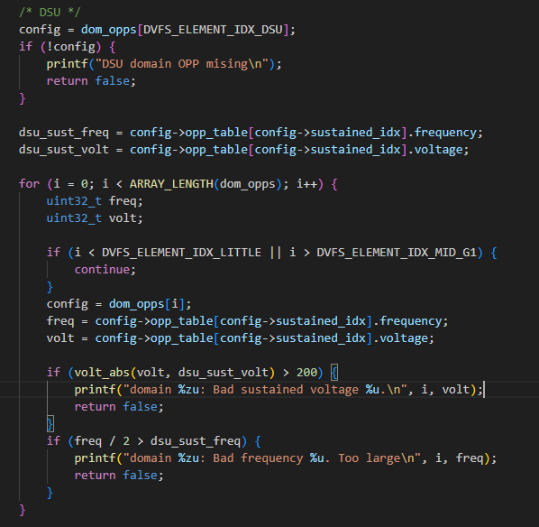
With DSU sustained levels being set to 1300 MHz and 790 mV, you are limited to 2600 MHz and 990 mV for the CPU blocks.
I have just realized the sanity check for frequency is wrong. It will always return TRUE for all CPU OPP tables because they only set the level field to indicate frequency.
I had tried bypassing the voltage check and increasing big cluster voltages up to 1.2 V, but it was still crashing. I’ll try to overclock the DSU block too and see how it goes.
@RadxaYuntian it would be nice if we could get some input from CIX on this stuff. I’m also curious about the absolute maximum ratings for core voltages.
@washley also made some good points above regarding differences between the big/medium “sub-clusters” (B0/B1, G0/G1).
Power draw was ~13 W at idle and occasionally went up to 50 W during the benchmark.
Unfortunately the B1 cluster heats up too much at 3.2 GHz and trips the thermal sensor (around 100 C?), shutting the board off. Not sure about the factory thermal paste but perhaps a Honeywell pad would do a better job.
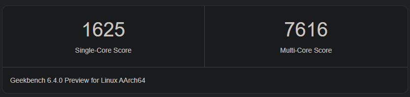
That’s pretty good, it doesn’t have to be ashamed in front of some x86. I’ll probably try to stick to 3.0+2.5 or something like this and start to undervolt the cores to figure what margin we have there and how much we can reduce the power draw. I also haven’t played with the “sustained” description, I suspect it will split the frequencies that are only accessible once the cpufreq “boost” is set but that’s pure speculation. If that was the case, we could add more opp that are not used by default, to ease with testing.
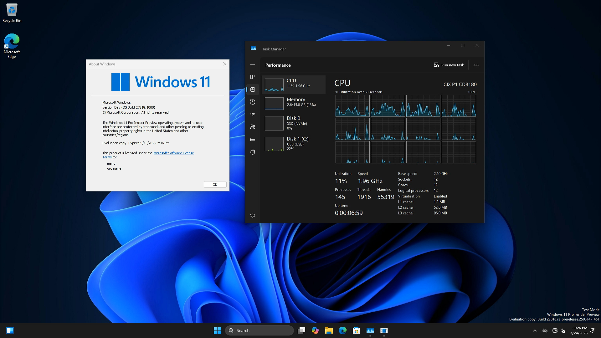
Got the latest insider build of Windows 11 (27818.1000) to boot with all cores.
It required a small kernel patch, though disabling the little cores would also work. These recent builds assume that all CPU cores support SPE, but it turns out that the A520s don’t, which leads to a fault when trying to access the missing CPU registers.
Usually no vendor supports overclocking, but given that the chip is currently configured to run a lower than advertised frequency, it’s reasonable to ask what should be the expected stable voltage for the original frequencies, and make sure what the limit not to cross is. They would definitely benefit from customers testing this. Look at RPi for example, whose stock frequencies have been increasing based on customer feedback. Here it would be perfectly possible that after 6 months they decide that 3 GHz is perfectly stable, and that becomes a nice marketing argument for them: first armv9-base SBC and first SoC running at 3 GHz stock.
Also it would be nice to know what causes the medium cores to have a lower limit than the other ones. Are they using a slightly different design which limits their frequency, is it a matter of power distribution on chip (e.g. cores located around the die have more power than those at the center), or is it purely arbitrary in order to limit the total capacity. Indeed, maybe some users would prefer to set all 8 cores at the same intermediary frequency and maintain a moderate wattage this way (e.g. 8x2.6 instead of 4x2.8 + 4x2.4, which would deliver the same total perf at less watts).
The original frequency is the design frequency, which once they taped it out, they realized that they could not reach it on all chips. The currently provided frequency is THE official stable frequency, and running above it is considered as overclocking. This is not to say that it can’t be changed in the future (we already see the memory speed increase), but for now, nobody knows where is the real limit.