Upgrade (Re-soldering) Memory on Rock 3A
(2GB → 8GB)
What I Needed:
- Soldering station – hot air gun for BGA soldering and a soldering iron with a BC2 (T12) tip or similar (portable options are possible). I also used a bottom preheater for the board.
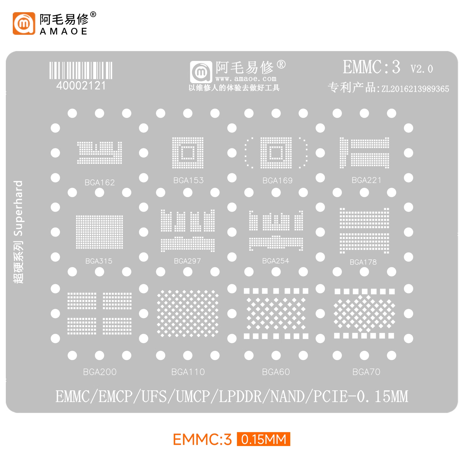
Universal Stencil for BGA200EMCP/UFS/UMCP/LPDDR (~$1.65)
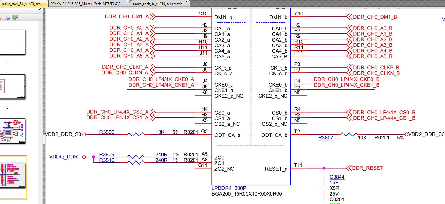
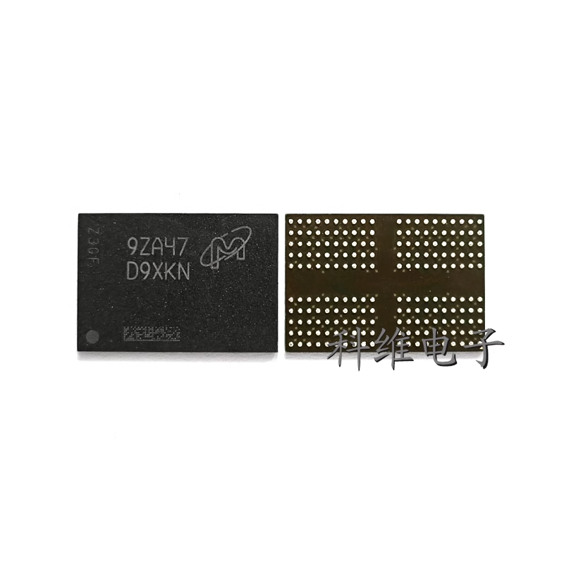
LPDDR4X Memory Chip D9XKN (8GB) (MT53E2G32D4DT-046) (~$15)
I already had solder paste (or BGA balls), BGA flux, solder, and other necessary consumables , so I didn’t buy them separately.
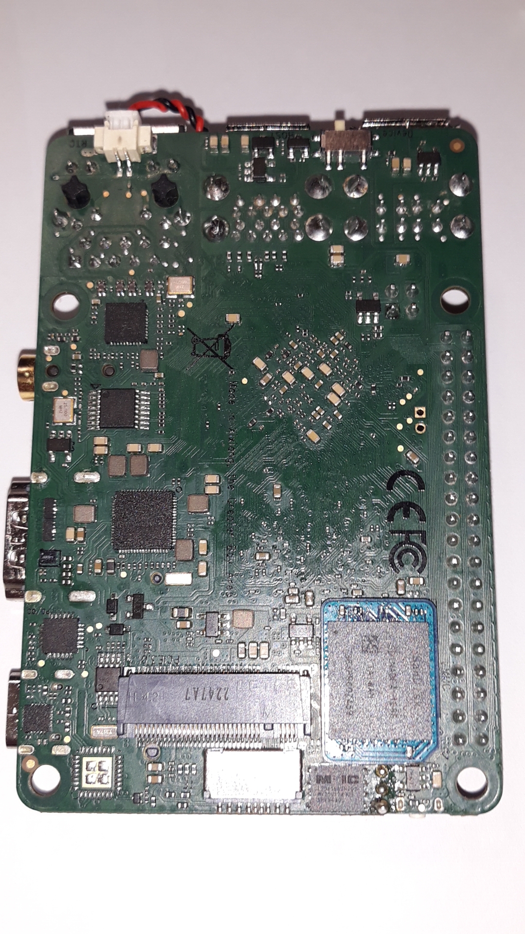
Additional Components for the Rock 3A SBC:
RTC Battery 3V (~$1)

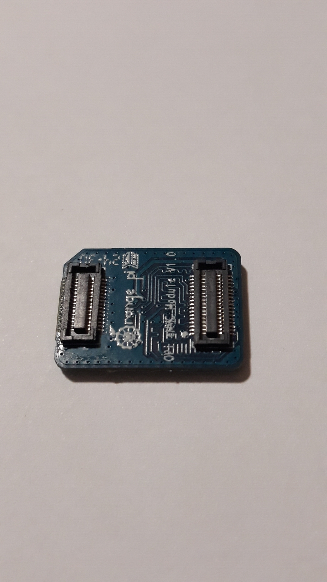
Blue eMMC Module (Orange PI 32GB) (~$6.2)
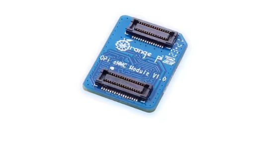
This confirms compatibility with Orange Pi eMMC modules . It is not necessary to buy a module specifically for Rock 3A. The Orange Pi eMMC module is also cheaper than the Rock eMMC version.
Purchasing and Shipping
I ordered the stencil and two types of memory chips from Taobao via a third-party forwarder. Since I was consolidating multiple purchases into a 1kg package , the shipping cost was significantly reduced . If you’re ordering from Taobao, consider additional expenses for forwarder shipping and delivery time.
Replacing the factory chip D9XRR (2GB) chip on the chip D9XKN (8GB) I got at the second attempt (apparently some balls rolled and shorted some lines just in this case and bought a stencil to once again do reboll chip), when LPDDR4 chip is missing (or it does not see the CPU as was in my case), the UART log output looks like this:
Error Log (LPDDR4 Not Detected)
DDR 2d653b3476 typ 24/01/20-15:04:19,fwver: v1.21
In
LP4/4x derate en, other dram:1x trefi
unknown device
error
ERR
(The system does not proceed further and hangs.)
Factory Memory Chip (D9XRR, 2GB) – UART Log Output
Summary
DDR 2d653b3476 typ 24/01/20-15:04:19,fwver: v1.21
In
LP4/4x derate en, other dram:1x trefi
ddrconfig:0
LPDDR4X, 324MHz
BW=32 Col=10 Bk=8 CS0 Row=16 CS=1 Die BW=16 Size=2048MB
tdqss: cs0 dqs0: -48ps, dqs1: -96ps, dqs2: -96ps, dqs3: -192ps,

change to: 324MHz
PHY drv:clk:36,ca:36,DQ:29,odt:0
vrefinner:24%, vrefout:41%
dram drv:40,odt:0
clk skew:0x64
rx vref: 26.4%
tx vref: 36.0%

change to: 528MHz
PHY drv:clk:36,ca:36,DQ:29,odt:0
vrefinner:24%, vrefout:41%
dram drv:40,odt:0
clk skew:0x58
rx vref: 28.4%
tx vref: 36.0%

change to: 780MHz
PHY drv:clk:36,ca:36,DQ:29,odt:60
vrefinner:16%, vrefout:41%
dram drv:40,odt:0
clk skew:0x58
rx vref: 16.6%
tx vref: 32.0%

change to: 1560MHz(final freq)
PHY drv:clk:36,ca:36,DQ:29,odt:60
vrefinner:16%, vrefout:22%
dram drv:40,odt:80
vref_ca:00000071
clk skew:0x30
rx vref: 15.6%
tx vref: 18.8%
cs 0:
the read training result:
DQS0:0x34, DQS1:0x34, DQS2:0x34, DQS3:0x31,
min  : 0xe 0x10 0x11  0xe  0x1  0x6  0xa  0x7 , 0xb  0x9  0x3  0x2  0xe  0xe  0xe  0xc ,
      0x10 0x10  0xd  0xa  0x3  0x2  0x3  0x7 , 0xc  0x8  0x7  0x2  0xe 0x10  0xc 0x14 ,
mid  :0x29 0x2a 0x2c 0x29 0x1d 0x21 0x25 0x23 ,0x26 0x24 0x1d 0x1d 0x29 0x28 0x29 0x27 ,
      0x2c 0x2b 0x27 0x25 0x1e 0x1d 0x1d 0x21 ,0x27 0x23 0x22 0x1d 0x29 0x2b 0x28 0x2e ,
max  :0x45 0x45 0x47 0x44 0x39 0x3d 0x40 0x3f ,0x42 0x40 0x38 0x39 0x45 0x42 0x44 0x42 ,
      0x48 0x47 0x41 0x41 0x3a 0x38 0x38 0x3c ,0x42 0x3e 0x3d 0x38 0x44 0x46 0x44 0x49 ,
range:0x37 0x35 0x36 0x36 0x38 0x37 0x36 0x38 ,0x37 0x37 0x35 0x37 0x37 0x34 0x36 0x36 ,
      0x38 0x37 0x34 0x37 0x37 0x36 0x35 0x35 ,0x36 0x36 0x36 0x36 0x36 0x36 0x38 0x35 ,
the write training result:
DQS0:0x27, DQS1:0x1d, DQS2:0x1d, DQS3:0xa,
min  :0x6e 0x72 0x73 0x70 0x63 0x67 0x6a 0x69 0x6a ,0x5e 0x5c 0x55 0x55 0x61 0x60 0x60 0x5f 0x5d ,
      0x67 0x65 0x60 0x5f 0x59 0x57 0x57 0x5d 0x5f ,0x54 0x50 0x4e 0x49 0x55 0x58 0x53 0x5a 0x50 ,
mid  :0x88 0x8c 0x8d 0x8a 0x7c 0x80 0x83 0x82 0x83 ,0x78 0x77 0x6f 0x6f 0x7c 0x7a 0x7a 0x79 0x76 ,
      0x83 0x81 0x7b 0x7a 0x73 0x71 0x72 0x77 0x79 ,0x6e 0x6a 0x68 0x62 0x71 0x72 0x6f 0x74 0x6b ,
max  :0xa2 0xa6 0xa8 0xa4 0x95 0x99 0x9d 0x9b 0x9c ,0x92 0x92 0x89 0x89 0x97 0x94 0x94 0x93 0x90 ,
      0x9f 0x9e 0x96 0x96 0x8e 0x8c 0x8d 0x92 0x94 ,0x89 0x84 0x82 0x7c 0x8d 0x8d 0x8b 0x8e 0x86 ,
range:0x34 0x34 0x35 0x34 0x32 0x32 0x33 0x32 0x32 ,0x34 0x36 0x34 0x34 0x36 0x34 0x34 0x34 0x33 ,
      0x38 0x39 0x36 0x37 0x35 0x35 0x36 0x35 0x35 ,0x35 0x34 0x34 0x33 0x38 0x35 0x38 0x34 0x36 ,
CA Training result:
cs:0 min  :0x49 0x45 0x3f 0x38 0x3d 0x35 0x40 ,0x49 0x42 0x3e 0x36 0x3b 0x37 0x40 ,
cs:0 mid  :0x86 0x86 0x7a 0x78 0x79 0x75 0x6d ,0x85 0x82 0x7a 0x75 0x77 0x77 0x6d ,
cs:0 max  :0xc3 0xc8 0xb6 0xb9 0xb6 0xb5 0x9b ,0xc2 0xc2 0xb6 0xb4 0xb4 0xb7 0x9b ,
cs:0 range:0x7a 0x83 0x77 0x81 0x79 0x80 0x5b ,0x79 0x80 0x78 0x7e 0x79 0x80 0x5b ,
out
...
...
After Replacing LPDDR4 with D9XKN (8GB) – UART Log Output
Summary
DDR 2d653b3476 typ 24/01/20-15:04:19,fwver: v1.21
In
LP4/4x derate en, other dram:1x trefi
ddrconfig:7
LPDDR4X, 324MHz
BW=32 Col=10 Bk=8 CS0 Row=17 CS1 Row=17 CS=2 Die BW=16 Size=8192MB
tdqss: cs0 dqs0: -24ps, dqs1: -96ps, dqs2: -72ps, dqs3: -168ps,
tdqss: cs1 dqs0: -24ps, dqs1: -96ps, dqs2: -72ps, dqs3: -168ps,

change to: 324MHz
PHY drv:clk:36,ca:36,DQ:29,odt:0
vrefinner:24%, vrefout:41%
dram drv:40,odt:0
clk skew:0x63
rx vref: 32.4%
tx vref: 40.0%

change to: 528MHz
PHY drv:clk:36,ca:36,DQ:29,odt:0
vrefinner:24%, vrefout:41%
dram drv:40,odt:0
clk skew:0x58
rx vref: 32.4%
tx vref: 38.0%

change to: 780MHz
PHY drv:clk:36,ca:36,DQ:29,odt:60
vrefinner:16%, vrefout:41%
dram drv:40,odt:0
clk skew:0x58
rx vref: 14.6%
tx vref: 32.0%

change to: 1560MHz(final freq)
PHY drv:clk:36,ca:36,DQ:29,odt:60
vrefinner:16%, vrefout:22%
dram drv:40,odt:80
vref_ca:00000071
clk skew:0x21
rx vref: 15.6%
tx vref: 21.8%
cs 0:
the read training result:
DQS0:0x2f, DQS1:0x2f, DQS2:0x30, DQS3:0x2a,
min  : 0xc  0xe 0x12  0xe  0x1  0x5  0xa  0x8 , 0x9  0x8  0x1  0x3  0xd  0xd  0xd  0xb ,
      0x10  0xf  0xa  0x9  0x1  0x3  0x2  0x5 , 0x9  0x7  0x6  0x1  0xf  0xe  0xb 0x12 ,
mid  :0x26 0x26 0x2a 0x26 0x1a 0x1e 0x22 0x21 ,0x21 0x1f 0x19 0x1c 0x26 0x24 0x25 0x22 ,
      0x29 0x28 0x22 0x21 0x1a 0x1a 0x19 0x1e ,0x22 0x1f 0x1d 0x19 0x27 0x26 0x24 0x29 ,
max  :0x40 0x3f 0x42 0x3f 0x34 0x37 0x3b 0x3a ,0x3a 0x37 0x32 0x35 0x3f 0x3b 0x3d 0x3a ,
      0x43 0x42 0x3b 0x3a 0x34 0x31 0x31 0x37 ,0x3c 0x37 0x34 0x32 0x3f 0x3f 0x3d 0x40 ,
range:0x34 0x31 0x30 0x31 0x33 0x32 0x31 0x32 ,0x31 0x2f 0x31 0x32 0x32 0x2e 0x30 0x2f ,
      0x33 0x33 0x31 0x31 0x33 0x2e 0x2f 0x32 ,0x33 0x30 0x2e 0x31 0x30 0x31 0x32 0x2e ,
the write training result:
DQS0:0x1d, DQS1:0xe, DQS2:0x13, DQS3:0x0,
min  :0x6a 0x6c 0x6f 0x6b 0x5d 0x63 0x65 0x65 0x65 ,0x54 0x52 0x4c 0x4c 0x58 0x58 0x56 0x55 0x54 ,
      0x5e 0x5e 0x59 0x59 0x52 0x50 0x52 0x56 0x58 ,0x4c 0x48 0x49 0x3e 0x4f 0x4f 0x4b 0x52 0x49 ,
mid  :0x83 0x86 0x8a 0x86 0x77 0x7c 0x7e 0x7d 0x7d ,0x70 0x6d 0x66 0x66 0x73 0x71 0x71 0x6f 0x6d ,
      0x7a 0x7a 0x73 0x73 0x6c 0x6a 0x6b 0x6f 0x71 ,0x66 0x61 0x61 0x59 0x6a 0x69 0x66 0x6b 0x62 ,
max  :0x9d 0xa1 0xa5 0xa1 0x91 0x95 0x98 0x96 0x95 ,0x8c 0x88 0x81 0x81 0x8e 0x8a 0x8c 0x8a 0x86 ,
      0x96 0x96 0x8e 0x8e 0x86 0x84 0x85 0x89 0x8a ,0x81 0x7b 0x79 0x75 0x85 0x84 0x81 0x85 0x7b ,
range:0x33 0x35 0x36 0x36 0x34 0x32 0x33 0x31 0x30 ,0x38 0x36 0x35 0x35 0x36 0x32 0x36 0x35 0x32 ,
      0x38 0x38 0x35 0x35 0x34 0x34 0x33 0x33 0x32 ,0x35 0x33 0x30 0x37 0x36 0x35 0x36 0x33 0x32 ,
cs 1:
the read training result:
DQS0:0x2f, DQS1:0x2f, DQS2:0x30, DQS3:0x2a,
min  : 0xc  0xe 0x12  0xe  0x1  0x5  0xa  0x8 , 0x9  0x8  0x1  0x3  0xd  0xd  0xd  0xb ,
      0x10  0xf  0xa  0x9  0x1  0x3  0x2  0x5 , 0x9  0x7  0x6  0x1  0xf  0xe  0xb 0x12 ,
mid  :0x26 0x26 0x2a 0x26 0x1a 0x1e 0x22 0x21 ,0x21 0x1f 0x19 0x1c 0x26 0x24 0x25 0x22 ,
      0x29 0x28 0x22 0x21 0x1a 0x1a 0x19 0x1e ,0x22 0x1f 0x1d 0x19 0x27 0x26 0x24 0x29 ,
max  :0x40 0x3f 0x42 0x3f 0x34 0x37 0x3b 0x3a ,0x3a 0x37 0x32 0x35 0x3f 0x3b 0x3d 0x3a ,
      0x43 0x42 0x3b 0x3a 0x34 0x31 0x31 0x37 ,0x3c 0x37 0x34 0x32 0x3f 0x3f 0x3d 0x40 ,
range:0x34 0x31 0x30 0x31 0x33 0x32 0x31 0x32 ,0x31 0x2f 0x31 0x32 0x32 0x2e 0x30 0x2f ,
      0x33 0x33 0x31 0x31 0x33 0x2e 0x2f 0x32 ,0x33 0x30 0x2e 0x31 0x30 0x31 0x32 0x2e ,
the write training result:
DQS0:0x1d, DQS1:0xe, DQS2:0x13, DQS3:0x0,
min  :0x6a 0x6c 0x6f 0x6b 0x5d 0x63 0x65 0x65 0x65 ,0x54 0x52 0x4c 0x4c 0x58 0x58 0x56 0x55 0x54 ,
      0x5e 0x5e 0x59 0x59 0x52 0x50 0x52 0x56 0x58 ,0x4c 0x48 0x49 0x3e 0x4f 0x4f 0x4b 0x52 0x49 ,
mid  :0x83 0x86 0x8a 0x86 0x77 0x7c 0x7e 0x7d 0x7d ,0x70 0x6d 0x66 0x66 0x73 0x71 0x71 0x6f 0x6d ,
      0x7a 0x7a 0x73 0x73 0x6c 0x6a 0x6b 0x6f 0x71 ,0x66 0x61 0x61 0x59 0x6a 0x69 0x66 0x6b 0x62 ,
max  :0x9d 0xa1 0xa5 0xa1 0x91 0x95 0x98 0x96 0x95 ,0x8c 0x88 0x81 0x81 0x8e 0x8a 0x8c 0x8a 0x86 ,
      0x96 0x96 0x8e 0x8e 0x86 0x84 0x85 0x89 0x8a ,0x81 0x7b 0x79 0x75 0x85 0x84 0x81 0x85 0x7b ,
range:0x33 0x35 0x36 0x36 0x34 0x32 0x33 0x31 0x30 ,0x38 0x36 0x35 0x35 0x36 0x32 0x36 0x35 0x32 ,
      0x38 0x38 0x35 0x35 0x34 0x34 0x33 0x33 0x32 ,0x35 0x33 0x30 0x37 0x36 0x35 0x36 0x33 0x32 ,
CA Training result:
cs:0 min  :0x45 0x37 0x39 0x2d 0x39 0x2a 0x3d ,0x45 0x36 0x38 0x2a 0x36 0x2a 0x3f ,
cs:0 mid  :0x7f 0x7d 0x74 0x71 0x72 0x6e 0x6a ,0x7e 0x7a 0x71 0x6c 0x6f 0x6e 0x6b ,
cs:0 max  :0xba 0xc3 0xb0 0xb5 0xab 0xb2 0x97 ,0xb8 0xbf 0xaa 0xaf 0xa9 0xb2 0x97 ,
cs:0 range:0x75 0x8c 0x77 0x88 0x72 0x88 0x5a ,0x73 0x89 0x72 0x85 0x73 0x88 0x58 ,
cs:1 min  :0x43 0x3b 0x37 0x30 0x37 0x30 0x3a ,0x40 0x37 0x37 0x2d 0x34 0x2f 0x3e ,
cs:1 mid  :0x7f 0x7c 0x74 0x6f 0x73 0x6e 0x6b ,0x7d 0x79 0x73 0x6d 0x70 0x6e 0x6b ,
cs:1 max  :0xbc 0xbe 0xb2 0xaf 0xb0 0xad 0x9c ,0xba 0xbc 0xaf 0xad 0xac 0xad 0x98 ,
cs:1 range:0x79 0x83 0x7b 0x7f 0x79 0x7d 0x62 ,0x7a 0x85 0x78 0x80 0x78 0x7e 0x5a ,
out
...
...
Benchmark Results
- Memory benchmark before upgrade:
 https://0x0.st/8ozz.bin
 - Memory benchmark after upgrade: https://0x0.st/8qGX.bin
Temperature and Power Consumption Increase
After the memory upgrade, I observed some important changes :
- Higher Temperature:
- With the factory 2GB D9XRR , the Rock 3A stayed cooler under load.
- The RK809 PMIC (Power Management IC) did not heat up significantly .
- However, after swapping the memory to D9XKN (8GB) , the PMIC became noticeably hotter under load (but not critically high ).
- Increased CPU Temps:
- The new LPDDR4 chip generates additional heat.
- Under load, the CPU temperature increased by +10°C :
- Before upgrade: Max 65°C (20°C at Room, Passive Heatsink)
- After upgrade: Max 75°C (20°C at Room, Passive Heatsink)
This increase is expected , as more memory requires higher power , causing higher heat dissipation from the voltage regulators.
Conclusion
Upgrading the Rock 3A from 2GB to 8GB RAM is possible with the right tools and patience. However, expect a slight increase in heat and power consumption . If you plan to do a similar upgrade, ensuring proper cooling would be a good idea.
(stress test was performed with the utility “stressapptest -s 1800 -i 4 -C 4 -W --stop_on_errors”, all memory utilization was more than 90%)
Datasheet - D9XKN-2412161825_Micron-Tech-MT53E2G32D4DT-046-AIT-A_C20552059.pdf
Datasheet - D9XRR-2410010333_Micron-Tech-MT53D512M32D2DS-046-WT-D_C22437469.pdf
Datasheet - H9HCNNNFAMMLXR(Rev.1.1)(1)(1)(1).pdf
Datasheet - 2411220416_Samsung-K4UCE3Q4AA-MGCL_C2920262.pdf
Datasheet - 2407151715_Samsung-K4UCE3Q4AB-MGCL_C29073172.pdf
Full DDR3L/DDR4/LPDDR4/LPDDR4x/LPDDR5 chip support file for different Rockchip RK3566/RK3568/RK3588/etc platforms:
Rockchip_Support_List_DDR_Ver2.56.pdf