
I’m interested in creating a carrier board for the CM3. Is there a mechanical drawing somewhere that I can use to create a Kicad footprint? (Or better yet, is there a Kicad footprint available?)
Mechanical drawings?
You can just use the RPi CM4 IO board Kicad project if you don’t need the third connector. The Radxa CM3 IO board is designed with Orcad and PADs.
I’m planning to use the third connector. I can make my own footprint if there’s a drawing somewhere with the location and orientation of the third connector.
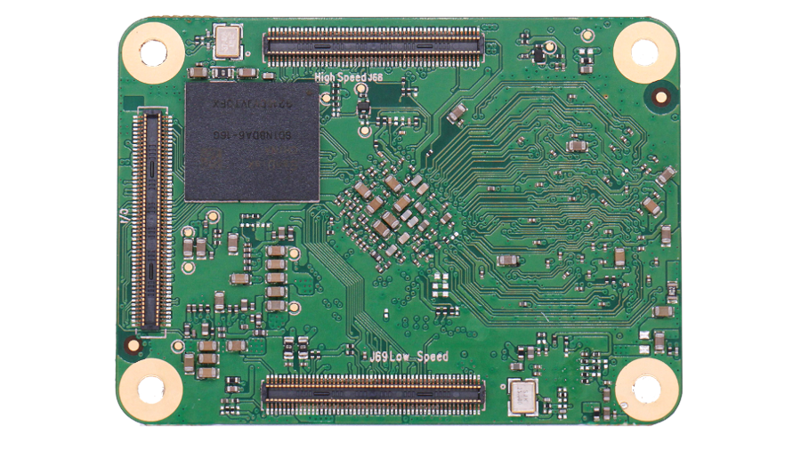
We have released the design of the Radxa CM3 IO board. Please check if there is anything missing.
1 Like
Perfect, thanks!
I’m having trouble finding software that can open the .pcb file. The .dxf file has pad placement, but doesn’t seem to have pad numbers / net names.
Can you tell me the order of the pads? Based on the 12 differential pairs on the bottom of the right side of the 3rd connector in this photo of the bottom of the CM3, it looks like 201 is the pin closest to the low speed connector. Is that correct?
You need:
OrCAD 16.6 or later, PADS 2.5VX or later.
to view the design files.
You can download a free version PADS viewer here:
Thank you, that’s helpful. However, I think you may have that upside-down. As you have it marked, pins 99, 93, 87, 81, 75, 69, 63, and 57 are all connected to the same copper pour (presumably GND.) - this is why I think those must be 1, 7, 13, 19, 25, 31, 37, and 43.
Hi there! Any luck designing that CM3 footprint for KiCad? I tired importing CM3 PDF, converted to dxf in inkscape, to footprint editor and aligning everything from there, but it’s not a precise reference (rectangles bigger than actual connectors). PDF seems to be in A4 format so definitely not to scale, and I had to scale it manually. Definitely not a good reference for such fine pitch connectors.
dxf files of cm3-io cannot be opened properly in neither inkscape nor kicad for any reason, it imports as a messy lump of text.
Any clues?  Thanks in advance!
We can try to convert the pcb to kicad, but not sure if the format will work 100%.
To be completely honest, if you published the coordinates of centers of all three connectors on the board, that would be enough information, and precise as well.
1 Like
I had some luck opening the DXF files in random online DXF to PDF converters, and was able to adapt the Raspberry Pi CM4 footprint to the CM3: https://github.com/EvanKrall/pipad/blob/radxa_cm3/footprints.pretty/Raspberry-Pi-4-Compute-Module.kicad_mod (this still has some die_length directives which may not be accurate for the CM3. Does the CM3 maintain the same relative lengths from pin to package as the CM4? See pages 23-26 in the CM4 datasheet.)
By the way, I think I’ve figured out what’s wrong with the pin numbering image you posted earlier: All of the pin numbers are correct relative to each other, but they’re arranged in the way they would be on the carrier board, looking down through the CM3. The image in the background is looking up at the bottom of the CM3. If the image of the CM3 were flipped top-to-bottom, it seems like this image would be accurate.
1 Like
I finally managed to get the PADS viewer running (had to set up a Windows VM first).
Here are the positions of the connectors on the CM3IO, based on averaging the center points of the top left and bottom right pins of each:
center of 3rd connector is x=(86.735+106.335)/2 = 96.535 , y=(81.69+84.33)/2 = 83.01
low-speed connector: x=(112.16 + 114.82) / 2 = 113.49, y=(71.285 + 51.685) / 2 = 61.485
high speed connector: x=(78.11 + 80.75)/2 = 79.43, y=(71.285 + 51.685) / 2 = 61.485
(96.535, 83.01)
(113.49, 61.485)
(79.43, 61.485)
drill holes:
- x=79.92, y=82.975
- x=112.92, y=82.975
- x=112.94, y=35.025
- x=79.94, y=35.025
(bottom two holes are shifted by 0.02mm compared to top two, apparently.)
2 Likes
RADXA Team - Did you ever create a Kicad footprint for the CM3? I’ve searched for it on your site, but all you have is the PADS file and DXF. I don’t have either, and Siemens is a PITA to get the PADS viewer from.
I need either a valid KICAD footprint or a dimensions that will allow me to create one, so I can order more…
I’ve got the connector footprint. If you don’t have a kicad footprint, and don’t want to create one, would you please just tell me the coordinates for the center of each hole and the center of pad 1 of each connector?
Respectfully,
MikeHagans